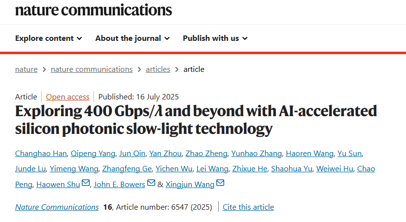
Recently, a joint team led by Professor Wang Xingjun and Research Fellow Shu Haowen from the Center, together with Academician John E. Bowers from the University of California, Santa Barbara (UCSB), has made a breakthrough in ultra-high-speed optical interconnects. They achieved, for the first time on a standard silicon photonics platform, an ultra-high-speed multi-channel signal transmission experiment at 400 Gbps per wavelength. The proposed AI-accelerated silicon slow-light modulation technology, based on a high-bandwidth all-silicon slow-light modulator chip and driven by an AI equalizer specifically designed for the nonlinear distortion of the silicon slow-light platform, significantly increased the single-wavelength transmission rate on a standard silicon photonics platform. This marks the world's first achievement of 400 Gbps per wavelength on a silicon-based platform and holds significant importance for the development of next-generation computing centers. On July 16th, the related research findings were published online in the Nature sub-journal Nature Communications under the title "Exploring 400 Gbps/λ and beyond with AI-accelerated silicon photonic slow-light technology".

Screenshot of the Article
With the rapid development of the information society, communication equipment and interconnect chips, as fundamental supporting infrastructure for the AI era and the digital economy, face pressure and challenges for upgrading their rates and capacities. To meet the demands for transmission rates and integration density driven by industry updates, silicon-based on-chip optical interconnects – leveraging advanced and mature microelectronics processes and fully utilizing the advantages of photonic technology such as high speed, multi-dimensionality, low latency, low energy consumption, and high parallelism – have become an inevitable trend in information technology development and a broad consensus in the industry. Silicon photonics technology enables the fabrication of photonic integrated chips using CMOS-compatible processes. By integrating micro/nano-optical devices on silicon substrates and leveraging the equipment, technology, and investment of the microelectronics industry, it facilitates the design, manufacture, and packaging of photonic integrated circuits, thereby reducing the manufacturing cost of optical chips. It has become a key supporting technology to meet future high-speed interconnects and massive computing power requirements. Consequently, based on low-cost, highly integrated silicon photonic chips, continuously improving transmission rates through structural and mechanistic optimization to satisfy the data throughput demands of data centers and high-performance computing interfaces has been a major research focus in the information and communication field in recent years.
For data center optical interconnect scenarios, Intensity Modulation/Direct Detection (IM/DD) systems, represented by four-level pulse amplitude modulation (PAM-4), modulate signals via optical intensity and are designated by IEEE standards as the technical route for short-reach optical interconnects due to their ease of deployment. However, due to the inherently slow carrier transport rate in silicon, the single-wavelength IM/DD transmission rates achieved in recent years using pure silicon modulators have shown a significant gap compared to the 400 Gbps per channel required for future ultra-fast optical interconnects, limiting the practical deployment of silicon photonics in ultra-fast interconnect scenarios.
To address these challenges, the research team proposed an innovative AI-accelerated silicon slow-light modulation technology, based on a high-bandwidth all-silicon slow-light modulator chip, to break through the current single-wavelength transmission rate limitations of silicon photonic platforms. The team employed CMOS-compatible standard silicon photonics processes to design and fabricate an eight-channel high-bandwidth wavelength-division multiplexing (WDM) silicon-based slow-light modulator chip operating around the 1550 nm communication wavelength, mitigating the inherent bandwidth-efficiency trade-off. Furthermore, utilizing a specifically designed AI equalizer targeting the nonlinear distortion of the silicon slow-light platform and based on the industry-standard high-order modulation format PAM-4, they achieved ultra-high-speed stable multi-channel signal transmission at the highest single-wavelength rate of 400 Gbps on a silicon photonic platform. The bit error rate (BER) remained below the HD-FEC threshold across the entire passband, achieving a total transmission capacity of 3.2 Tbps and an on-chip data rate density of up to 1.6 Tb/s/mm². This demonstrates the applicability of the silicon photonics solution in the ultra-fast interconnect field. Without introducing heterogeneous materials or complex processes, this scheme significantly enhances the single-wavelength transmission rate on an all-silicon material platform using an industry-standard format, fully leveraging the industrialization advantages of silicon photonics and achieving deep integration of silicon photonics and AI technology. This achievement validates the immense value of silicon photonics in next-generation 3.2 TbE optical interconnects and experimentally demonstrates the high compatibility between silicon photonic platforms and AI-driven solutions in the context of AI for Science (AI4S). It is expected to be applied in next-generation computing centers, providing new ideas for on-chip optical interconnect solutions and accelerating AI industry upgrades.

AI-Accelerated Silicon-Based Slow-Light Modulation Technology
The co-first authors of the paper are Dr. Han Changhao (Postdoctoral Researcher at UCSB & PhD from the Center), Yang Qipeng (PhD candidate at the Center), Associate Professor Qin Jun (Beijing Information Science & Technology University), and Associate Research Fellow Zhou Yan (Yangtze Delta Institute of Optoelectronics, Peking University). Professor Wang Xingjun and Research Fellow Shu Haowen from the Center, and Academician John E. Bowers from UCSB are the corresponding authors. Academician Yu Shaohua from Peng Cheng Laboratory participated in the work and provided important guidance. Major collaborators also include Professor Peng Chao and Professor Hu Weiwei from the School of Electronics at Peking University, Dr. Zheng Zhao (PhD graduate), PhD candidates Wang Yimeng and Wu Yichen; Researcher He Zhixue and Researcher Wang Lei from Peng Cheng Laboratory, PhD candidates Zhang Yunhao and Wang Haoren; Associate Research Fellow Ge Zhangfeng from the Yangtze Delta Institute of Optoelectronics, Peking University; and Master's candidates Sun Yu and Lü Junde from Beijing Information Science & Technology University. The work was completed with the National Key Laboratory of Photonic Transmission and Communication at the School of Electronics, Peking University, as the primary affiliation.
Link to the original paper: https://www.nature.com/articles/s41467-025-61933-5

